From schematic to PCB mainboard
A motor-drive circuit drawn as power, control and feedback sections, then laid out as a board with copper traces and parts, the way a PCB design takes shape.
Engineering Service
Project-based PCB design and board layout for custom industrial electronics, with deliverables and scope agreed for each job.
Overview
Custom industrial electronics projects need a board designed around the actual requirement — interfaces, space, power and the environment it will work in.
We provide PCB design and board-layout services, working from your project requirements to develop the board design and layout. Deliverables and technical scope are agreed for each job.
Past projects
A selection of PCBs we designed in-house, from schematic to board layout, for customers' equipment in wafer fabs. Customer names, sites and part numbers are not shown.
Illustrative 3D model drawn in code to explain how the build works. Not a photograph.
Control card redesign
A control card for an electroplating machine: a 136 × 183 mm plug-in card with a 22-way, 3.96 mm edge connector. We designed it as a through-hole board, then redesigned it as an SMD assembly that keeps the same edge-connector pinout, so the new card fits the same slot.
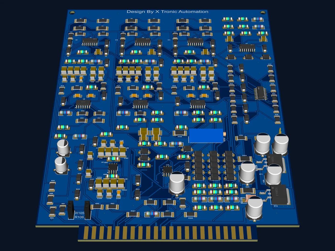
Illustrative 3D model drawn in code to explain how the build works. Not a photograph.
Interface board
Two 2 × 20 headers wired pin for pin, so two 40-way ribbon cables join straight through.
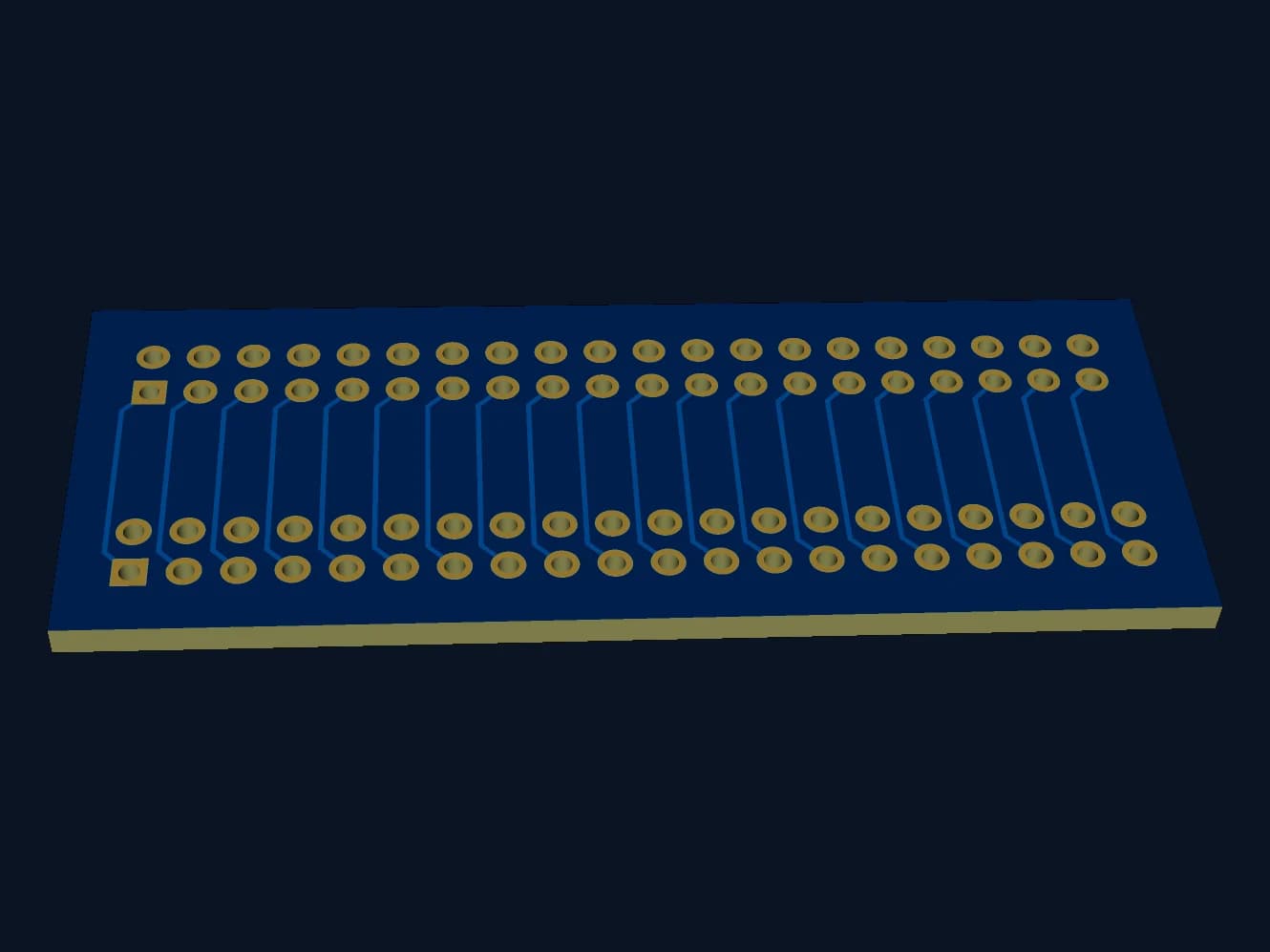
Illustrative 3D model drawn in code to explain how the build works. Not a photograph.
LED board
64 LEDs in 16 strings: each string is four LEDs in series with its own 47 Ω resistor, and the strings are wired in parallel in two banks of eight.
Illustrative 3D model drawn in code to explain how the build works. Not a photograph.
Interface board
Breaks a 9-way D-sub plug out to rows of solder pads for wiring into a machine.
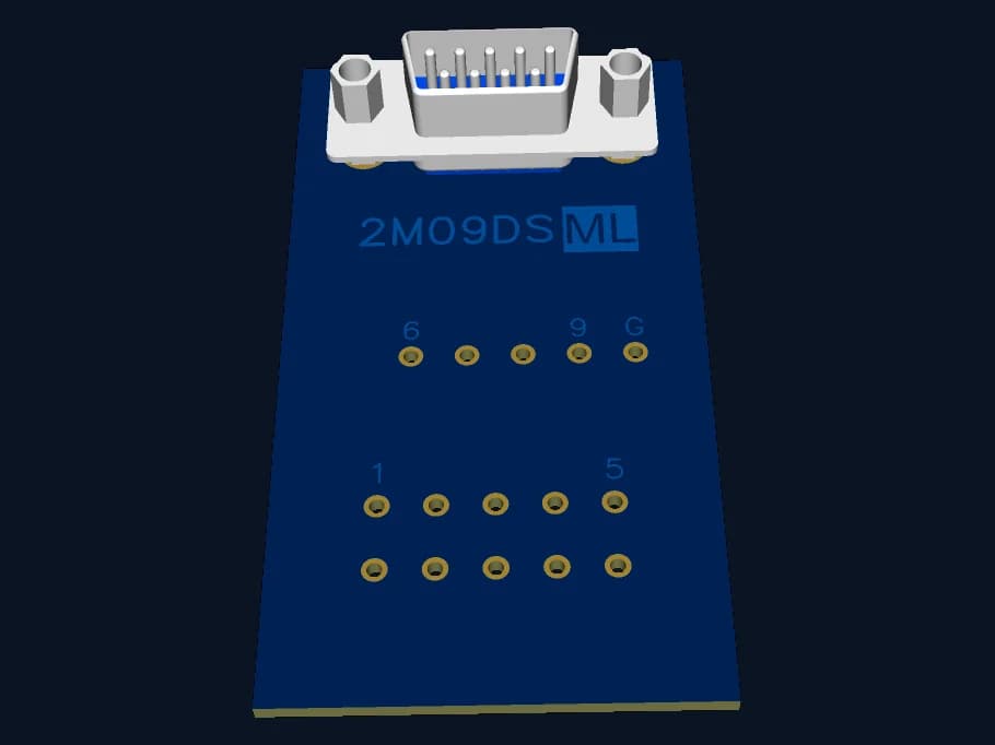
Illustrative 3D model drawn in code to explain how the build works. Not a photograph.
Interface board
Combines a 5-way and a 4-way wire-to-board connector into one 9-way connector, so two cables can plug into equipment that takes one.
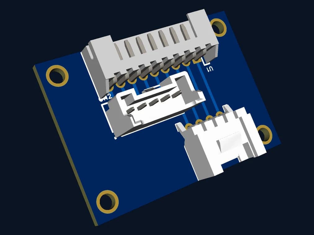
In 3D
A motor-drive circuit drawn as power, control and feedback sections, then laid out as a board with copper traces and parts, the way a PCB design takes shape.
Illustrative models drawn in code. Not photographs of customer equipment or of a specific product.
Applicable equipment
Send the brand, model and part number with photographs, and we will review whether the unit is within our repair scope.
Typical faults
Engineering process
Review the project requirements and intended application.
Clarify interfaces, constraints and information available.
Confirm deliverables, technical scope and quotation.
Develop the board design and layout.
Deliver the agreed design outputs.
Verification depends on the equipment and available test conditions. Workshop checks are distinguished from testing that requires your machine, program or production setup.
Request for Quotation
Share the manufacturer, model or part number, quantity and the fault you are seeing. Photos or documents help us assess the job faster.