Capability area 11 / 11
PCB design & layout
PCB design and board-layout services for custom industrial electronics projects, developed from the project requirements with deliverables and technical scope agreed for each job.
- PCB design
- Board layout
- Project-based development
3D model above is illustrative and drawn in code. Not a photograph of customer equipment or of a specific product.
Past projects
Boards we have designed
A selection of PCBs we designed in-house, from schematic to board layout, for customers' equipment in wafer fabs. Customer names, sites and part numbers are not shown.
Illustrative 3D model drawn in code to explain how the build works. Not a photograph.
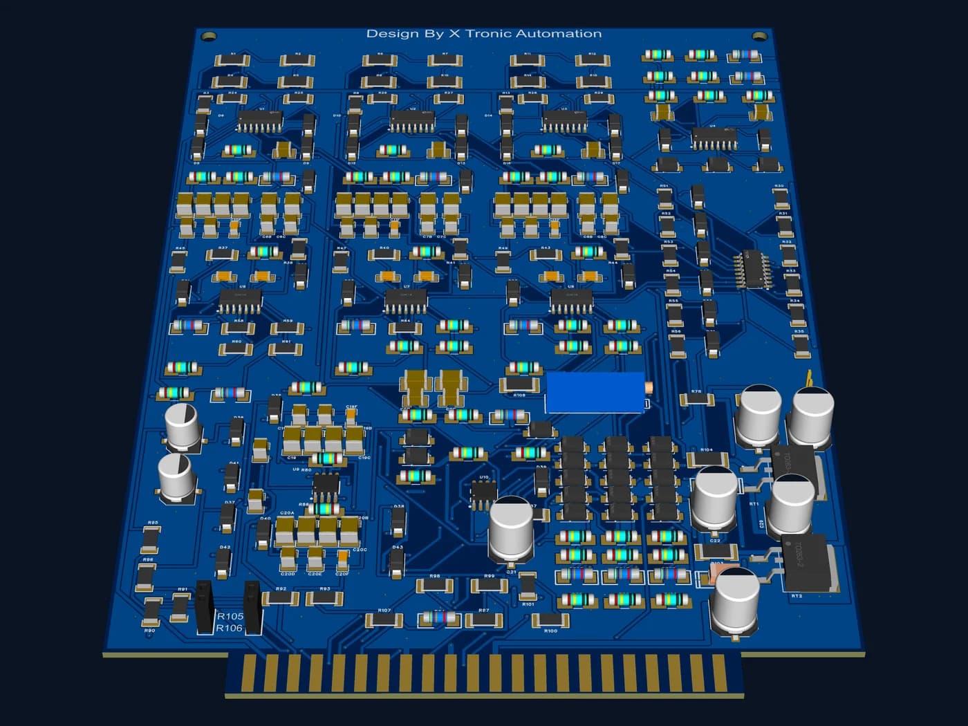
Control card redesign
Three-channel firing board, through-hole to SMD
A control card for an electroplating machine: a 136 × 183 mm plug-in card with a 22-way, 3.96 mm edge connector. We designed it as a through-hole board, then redesigned it as an SMD assembly that keeps the same edge-connector pinout, so the new card fits the same slot.
- On-board regulators for the ±12 V rails
- Phase reference inputs, three timing channels and three output drivers
- Firing point set against an adjustable control level, trimmed on the board
- SMD revision keeps every original terminal connection
- Odd component values built from stocked parts, for example 22 kΩ as 10 kΩ + 10 kΩ + 2 kΩ
3D render from our design files Illustrative 3D model drawn in code to explain how the build works. Not a photograph.
Interface board
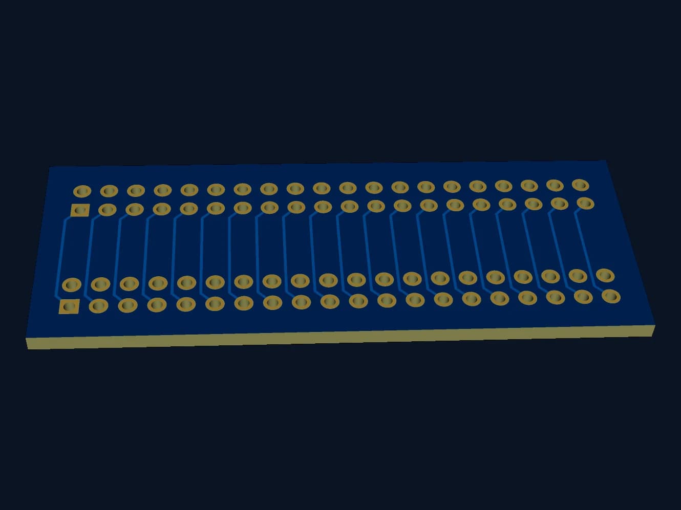
40-pin pass-through adapter
Two 2 × 20 headers wired pin for pin, so two 40-way ribbon cables join straight through.
- Every pin on one header goes to the same pin on the other
- Odd pins routed on the top layer, even pins on the bottom layer
- Pin 1 marked with a square pad on both headers
- Two mounting holes
3D render from our design files Illustrative 3D model drawn in code to explain how the build works. Not a photograph.
LED board
LED lighting board
64 LEDs in 16 strings: each string is four LEDs in series with its own 47 Ω resistor, and the strings are wired in parallel in two banks of eight.
- One current-limiting resistor per string
- If one LED fails, only its own string goes out
- Two-way supply terminal in the middle of the board
Illustrative 3D model drawn in code to explain how the build works. Not a photograph.
Interface board
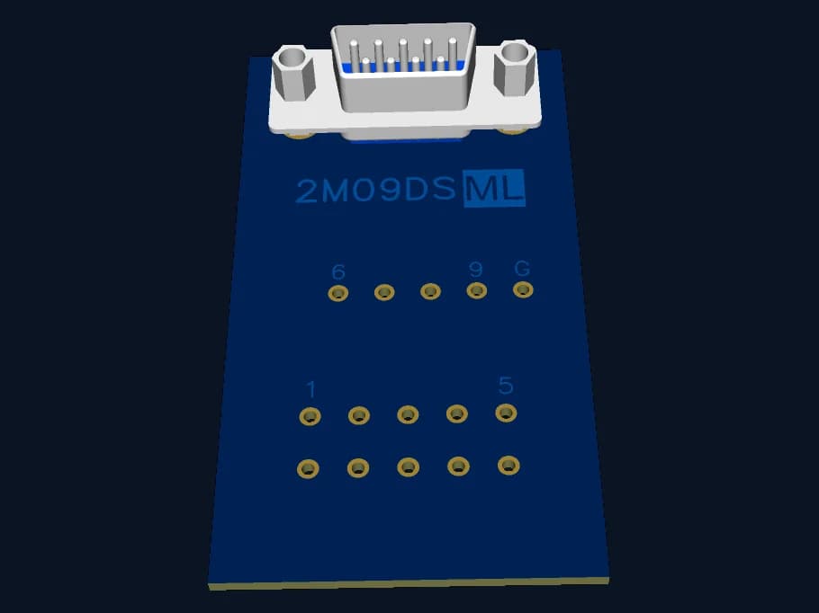
DB9 breakout board
Breaks a 9-way D-sub plug out to rows of solder pads for wiring into a machine.
- Right-angle D-sub on the board edge, with jack screws
- Pins 6 to 9 and the shell ground on one row
- Pins 1 to 5 on two linked rows, so each signal can be picked up twice
- Wide ground track from the connector shell
3D render from our design files Illustrative 3D model drawn in code to explain how the build works. Not a photograph.
Interface board
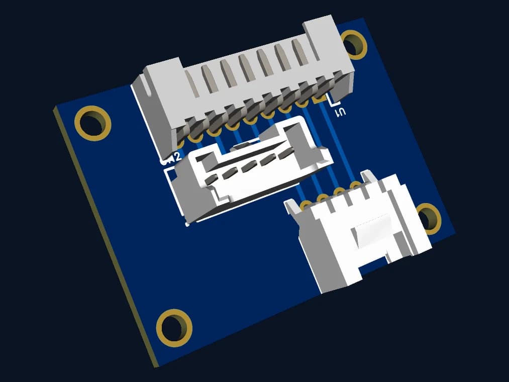
5 + 4 to 9-way connector adapter
Combines a 5-way and a 4-way wire-to-board connector into one 9-way connector, so two cables can plug into equipment that takes one.
- 5-way input to pins 9 to 5, 4-way input to pins 4 to 1
- Short, straight tracks between the connectors
- Mounting hole in each corner for standoffs
3D render from our design files
Request for Quotation
Request a quotation: PCB design & layout
Share the manufacturer, model or part number, quantity and the fault you are seeing. Photos or documents help us assess the job faster.